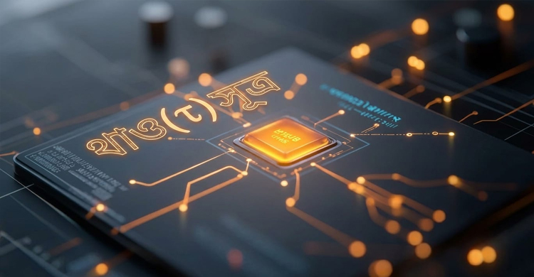
| International Desk: A newly proposed semiconductor development model known as the “Tau (τ) Law” has quickly become a major topic of discussion across the global technology industry. Introduced by He Tingbo, President of Huawei’s Semiconductor Business Group, the concept is being presented as a potential successor—or complement—to the long-dominant Moore’s Law, with implications that could significantly influence technology and daily life over the next decade.
What Is the Tau Law?
For more than half a century, the semiconductor industry has largely followed Moore’s Law, first proposed by Intel co-founder Gordon Moore. The principle suggests that the number of transistors on a chip doubles approximately every 18 to 24 months, delivering greater computing power while keeping costs relatively stable.
For decades, chipmakers improved performance primarily by shrinking transistor sizes. However, as manufacturing processes approach physical limitations, further miniaturization has become increasingly difficult and expensive.
Industry experts note that producing chips below the 3-nanometer threshold requires enormous investments. Building a cutting-edge 3-nanometer fabrication plant can cost tens of billions of dollars, while a single EUV lithography machine may cost hundreds of millions. These expenses are often reflected in the prices consumers pay for advanced electronic devices.
The Tau Law proposes a different path. Rather than focusing solely on shrinking transistors, it emphasizes improving efficiency through what Huawei describes as “time compression” and “logic folding.”
Logic folding aims to overcome the limitations of traditional two-dimensional chip layouts by reorganizing circuits into multi-layered structures. This approach shortens signal transmission paths, reduces energy losses, and enhances overall efficiency without relying exclusively on ever-smaller transistors.
A New Way of Thinking About Performance
Supporters of the concept often compare a chip to a city’s transportation network.
Under the traditional model, improving performance resembles adding more vehicles and roads to increase traffic capacity. Eventually, however, congestion becomes unavoidable.
The Tau Law approach focuses instead on improving traffic flow—through better road design, overpasses, optimized routing, and smarter coordination—allowing the system to move more efficiently without simply increasing density.
Applied to semiconductors, the goal is to achieve higher performance through architectural optimization rather than relying entirely on transistor miniaturization.
What Could It Mean for Consumers?
If such technologies prove successful at scale, they could help reduce the cost of delivering high-performance computing.
According to Huawei, advanced processing capabilities may eventually be achieved using more mature manufacturing technologies, potentially lowering production costs for products such as smartphones, computers, and other electronic devices.
The company says it has already applied Tau Law-related concepts in the design and production of hundreds of chip products over the past six years. Huawei also plans to introduce more extensive logic-folding technologies in future Kirin mobile processors.
The company estimates that by 2031, chips based on these concepts could achieve performance densities comparable to far more advanced manufacturing nodes while potentially reducing costs.
Implications for Artificial Intelligence
The impact could extend well beyond consumer electronics.
Because the Tau Law focuses on improving efficiency and reducing end-to-end processing time, it could lower the computational costs associated with artificial intelligence applications.
This may allow AI systems to operate more efficiently on local devices rather than relying exclusively on cloud-based infrastructure. Future smartphones, home appliances, and vehicles could potentially incorporate more advanced AI capabilities while consuming fewer resources.
Lower chip costs and improved performance could also contribute to wider adoption of intelligent driving technologies, making advanced driver-assistance systems accessible in more affordable vehicles rather than being limited to premium models.
A New Direction for the Semiconductor Industry?
Proponents argue that the Tau Law reflects a broader shift in thinking within the semiconductor sector. Instead of viewing cutting-edge nanometer manufacturing as the sole measure of progress, the approach emphasizes system-level optimization, architectural innovation, and practical efficiency gains.
Supporters believe this could offer an alternative pathway for future semiconductor development and contribute to the evolution of next-generation AI and computing technologies.
While the concept remains relatively new and its long-term impact has yet to be fully assessed by the global scientific and engineering community, the Tau Law has already sparked debate about the future direction of chip design and whether innovation beyond transistor scaling may define the next chapter of technological advancement.
Source: Swarna, Touhid and Lili, China Media Group (CMG).
|